
More RAM
Today I managed to get FPGABee's memory bank switching working and it now has the full 128K.
Getting the RAM Off-chip
Previously FPGABee's main RAM was implemented as a single on-chip (ie: in the FPGA chip) 32K block RAM. While this worked well for version 1, the Spartan chip I'm using has a total of about 60K RAM available so it was time to move it off-chip and start using the Nexys-3 board's SDRAM - of which it has 16MB.
Interfacing to the SDRAM is almost identical to interfacing to the flash memory and in fact they both share the same address and data lines. Switch to the external RAM basically involved some minor changes to the address decoding and data multiplexing logic and deleting the old block RAM entity.
To verify this was all working I booted the old ROM Basic and ran up a couple of programs and everything worked fine.
Understanding the Premium 128K's Memory Banking
The biggest challenge to implementing the full 128K of RAM was understanding how the bank switching worked. With a total address space of 64K obviously the full 128K can't all be accessible at once and the key to all this is understanding how port 0x50 works. Unfortunately the official documentation for this is not quite correct, but managed to figure it out by reviewing the source code for ubee512 and some testing.
The 128K of RAM is divided into 4 banks of 32K and the banks are selected according to port 0x50:
- Bit 0-1 - Selects which of the 4 32K banks appears at 0x0000-0x8000 (but see note below)
- Bit 2 - When 1 deselects all ROM packs from memory. When 0, ROM pack 1 appears at 0x8000-0xBFFF and bit 5 controls the other ROM packs.
- Bit 3 - When 1 deselects all video memory from memory
- Bit 4 - When 0, video memory appears at it's normal location 0xF000-0xFFFF. When 1, video memory appears at 0x8000-0x8FFF
- Bit 5 - When 0, ROM pack 2 appears at 0xC000 to 0xFFFF. When 1, ROM pack 3 appears at 0xC000 to 0xFFFF
Well that's how it's documented in the technical reference manual however they neglected to mention one thing: when bit 2 is set the meaning of bit 1 is inverted. I don't know why, but that's how it is.
Also, bank 0 is always mapped to 0x8000-0xFFFF unless obstructed by another of the other mapping defined above.
Fixing the Address Decoding and Data Multiplexing
Once I had my head around how port 0x50 worked I took a look at FPGABee's existing implementation of memory mapping and decided it was getting a bit out of hand. I had multiple places that were decoding addresses, a huge continuous assignment statement for the CPU din signals and it was just getting too unwieldy.
After a bit of a redesign I came up with a structure that make the whole thing more manageable. Firstly, instead of using continuous assignment statements I used VHDL non-clock processes - allowing for more explicit if/elsif declarations of the logic.
Secondly I consolidated all the address decoding to single place that decodes the current CPU address to a device (eg: ram, rom, video character ram, video pcg ram etc...) and a "translated address" - the address in the target device that the current CPU address maps to. Normally the translated address is the same as the CPU address with the top few bits cropped off (eg: the video ram is simply the bottom 12 bits of the CPU address). For ROM access however it's offset to the base location in the flash memory of where the ROM image resides. For RAM access it's offset according to the selected bank number.
Bringing it all together gives the following address decoding logic. It's complicated but at least it's clearly stated:
-- Map z80 addresses
process (z80_addr, port_50, port_1c, port_08, latch_rom, small_char_set_selected, mem_rd, pcu_mode)
begin

	ram_range <= '0';
	rom_range <= '0';
	char_ram_range <= '0';
	attr_ram_range <= '0';
	pcg_ram_range <= '0';
	color_ram_range <= '0';
	charrom_range <= '0';

	-- Default translated address
	translated_address <= "00000000000" & z80_addr;

	if port_50(3)='0' and 											-- Video RAM enabled
		((port_50(4)='0' and z80_addr(15 downto 12)=x"F") or			-- 0xF000 - 0xFFFF
		 (port_50(4)='1' and z80_addr(15 downto 12)=x"8")) then		    -- 0x8000 - 0x8FFF

		if z80_addr(11)='0' then

			if latch_rom='0' then

				-- Lower video RAM
				if port_1c(4)='0' then
					char_ram_range <= '1';
				else
					attr_ram_range <= '1';
				end if;

			else

				translated_address <= "000000000000000" & small_char_set_selected & z80_addr(10 downto 0);
				charrom_range <= '1';

			end if;

		else

			-- Upper video RAM
			if port_08(6)='0' then

				pcg_ram_range <= '1';
				if port_1c(7)='1' then

					-- Extended PCG banks enabled
					translated_address <= "0000000000000" & port_1c(2 downto 0) & z80_addr(10 downto 0);
					pcg_ram_range <= not port_1c(3);  -- if accessing >16K PCG ram, ignore/return 0

				else

					-- Extended PCG banks disabled
					translated_address <= "0000000000000" & "000" & z80_addr(10 downto 0);

				end if;
			else

				color_ram_range <='1';

			end if;
		end if;

	elsif port_50(2)='0' and z80_addr(15)='1' then

		-- ROM Range
		rom_range <= '1';

		if z80_addr(14)='0' then 		-- < 0xC000

			-- ROM 1 0x8000->0xBFFF (comes from flash 0x100000 -> 0x103FFF)
			translated_address <= rom_base_address(26 downto 16) & "00" & z80_addr(13 downto 0);

		elsif port_50(5)='0' then

			-- ROM 2 0xC000->0xFFFF (comes from flash 0x104000 -> 0x107FFF)
			translated_address <= rom_base_address(26 downto 16) & "01" & z80_addr(13 downto 0);

		else

			-- ROM 3 0xC000->0xFFFF (comes from flash 0x108000 -> 0x10BFFF)
			translated_address <= rom_base_address(26 downto 16) & "10" & z80_addr(13 downto 0);

		end if;

	elsif z80_addr(15)='1' then

		-- RAM access above 0x8000 is always to bank 0 block 0
		ram_range <= '1';
		translated_address <= "0000000000" & "00" & z80_addr(14 downto 0);

	else

		-- Banked RAM access
		-- NB: when port50 bit 2 is set, the meaning of port50 bit 1 is inverted - hence the xor below
		ram_range <= '1';
		translated_address <= "0000000000" & (port_50(1) xor port_50(2)) & port_50(0) & z80_addr(14 downto 0);

	end if;

end process;
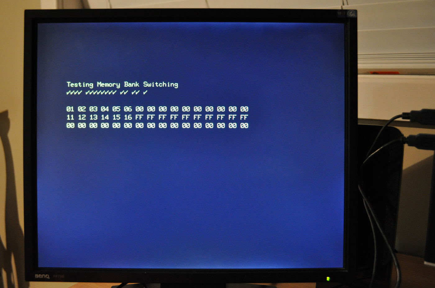
Testing
Again, testing this wasn't possible with full system boot so I knocked together another boot ROM to check everything looked correct. By running the test ROM on ubee512 and on FPGAbee I could confirm they were both doing the same thing.
Each tick represents a passed test.
Getting Closer
Next up is the disk controller.