A Simple On-Chip Logic Analyzer for FPGAs
A simple on-chip logic analyzer written in VHDL, using NodeJS for data capture and GtkWave for analysis.
Recently I was struggling to get the LPDDR RAM on a Mimas V2 board to work with my FPGA TRS-80. With no insight into what was going on I knocked together this simple VHDL/NodeJS/GtkWave based logic analyzer - and it works much better than expected.
In a previous post I covered a similar component called Reflector that can mirror a set of signal values from the FPGA back to a connected PC via a serial connection. That component was designed as an alternative to on-board UI elements like LEDs and seven segment displays. While similar to a logic analyzer in that it captures signal values and transmits them to a PC, it runs far too slowly to be used as a logic analyzer.
LogicCapture re-uses much of the Reflector's implementation but is designed for use as a logic analyzer:
- Reflector captures signals indefinitely and transmits them as quickly as possible - but will drop transitions that happen while busy transmitting.
- LogicCapture captures as many signal samples will fit in the allocated RAM - and then transmits the entire buffer to the PC.
In other words LogicCapture captures every signal transition - but only for a small slice of time.
Embedding the LogicCapture Component
The first step to using this component is to embed the LogicCapture component into your VHDL design. (source here, it uses a few other components all of which are in the same folder)
	cap : entity work.LogicCapture
	generic map
	(
		p_clock_hz => 80_000_000,
		p_baud => 115200,
		p_bit_width => 55,
		p_addr_width => 11
	)
	port map
	(
		i_clock => s_clock_80mhz,
		i_clken => s_clken_cpu,
		i_reset => s_reset,
		i_trigger => s_logic_trigger,
		i_signals => s_logic_capture,
		o_uart_tx => o_uart_tx
	);
The parameters and signals are as follows:
p_clock_hz- the frequency of thei_clocksignal (used to calculate correct baud rate timing).p_baud- the baud rate to transmit at.p_bit_width- the number of logic bits to be captured in each sample.p_addr_width- the size of the RAM capture buffer. The number of samples captured will be2^p_addr_width.i_clock- the system clock (all other signals are synchronous to this).i_clken- an optional clock enable. Samples will be captured when this signal is asserted and intervening samples will be discarded.i_reset- synchronous, active high reset.i_trigger- capture starts when this signal is asserted.i_signals- the signals to be captured.o_uart_tx- generated serial signal that should be routed to the listening PC.
Most of the above is self explanatory. For details on the serial connection to the PC, see the post about the Reflector component.
Data capture begins when the i_trigger input is asserted and continues until memory runs out. To trigger a subsequent capture you need to first reset the component withi_reset. Alternatively you can tie i_trigger to 1 and use i_reset to trigger a new capture.
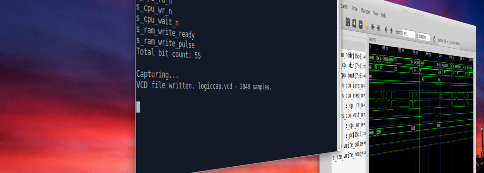
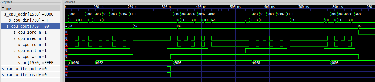
Next you need to assign your input signals and the trigger signal. In this example I was trying to debug the memory interface between a Z-80 soft core and the board's DDR RAM so I'm capturing most of the Z-80 bus signals and I use the memory controllers "calibration done" signal to trigger the start of the capture since I wasn't interested in anything before then.
	signal s_logic_capture : std_logic_vector(54 downto 0);
	signal s_logic_trigger : std_logic;

    .
    .
    .

    s_logic_capture <=
		s_pc & s_cpu_addr & s_cpu_din & s_cpu_dout
		& s_cpu_mreq_n & s_cpu_iorq_n
		& s_cpu_rd_n & s_cpu_wr_n & s_cpu_wait_n
		& s_ram_write_ready & s_ram_write_pulse
		;
	s_logic_trigger <= s_calib_done;
Note:
s_logic_captureis declared with the same width as thep_addr_widthparameter and combines together all the signals to be analyzed.s_logic_triggercan be tied to1to capture from the start.
Running the Capture Script
To receive the data transmitted from the FPGA, I've written a NodeJS script that listens on the serial port and generates a .vcd file. Run it as follows:
$ node logiccap --port:/dev/ttyACM1 --baud:115200 --sampleRate:1774000 --autoview:150 s_pc[16] s_cpu_addr[16] s_cpu_din[8] s_cpu_dout[8] s_cpu_mreq_n s_cpu_iorq_n s_cpu_rd_n s_cpu_wr_n s_cpu_wait_n s_ram_write_ready s_ram_write_pulse
That's a lot of stuff, let's break it down:
node- launches the NodeJS executablelogiccap- the name of the node script (get it here)--port:/dev/ttyACM1- the serial port to listen to--baud:115200- the serial baud rate (must match LogicCapture'sp_baudparameter)--sampleRate:1774000- the sample rate of the data. Used to calculate correct timestamp values for the .vcd file. This should match the frequency of thei_clkensignal.--autoview:150- automatically launches GtkWave to view the .vcd file if more that 150 valid samples are received.
The rest of the parameters are the signal declarations that must match what you've assigned to the LogicCapture's i_signals port. The square bracketed numbers declare the signal's bit width (if omitted it's assumed to be a single bit signal).
The --autoview parameter takes a minimum sample count since sometimes on re-programming a FPGA board a small number of samples can be sent when the board is reset during programming. Setting this threshold prevents the script from launching GtkWave for those spurious samples.
Obviously you're not going to want to type all of that every time so I recommend either setting up a script to launch it or I prefer to use a makefile target like so:
capture:
	@node ../../../fpgakit/tools/reflector-client/logiccap \
	--port:/dev/ttyACM1 \
	--baud:115200 \
	--sampleRate:1774000 \
	--autoview:150 \
	s_pc[16] \
	s_cpu_addr[16] \
	s_cpu_din[8] \
	s_cpu_dout[8] \
	s_cpu_mreq_n \
	s_cpu_iorq_n \
	s_cpu_rd_n \
	s_cpu_wr_n \
	s_cpu_wait_n \
	s_ram_write_ready \
	s_ram_write_pulse
You can then launch it with a simple make capture command.
All Set
That's everything now setup and ready to go.
- Upload your design to the FPGA board
- When triggered the script will display "Capturing..."
- After a short delay, GtkWave will be launched and you can inspect the results.
The script will also keep running and listening for more updates. Reset the board and you'll automatically get another capture and GtkWave launched again.
(Note the script assumes gtkwave is on your path)
Here's a video walk-through showing it in action:
Wrap Up
There are a number of pros and cons to this approach:
Pros:
- Extremely simple, could be customized if needed
- Very small capture engine uses minimal FPGA resources
- Doesn't require any additional hardware
- Doesn't require routing signals to external pins for probes to be connected.
- Can capture more signals than a traditional logic analyzer (I've used this to capture over 130 signals)
- Only requires a single external wire connection for the serial transmission
- Captured samples are synced precisely to your design's clock so oversampling isn't needed to capture every sample
- The trigger condition can be as complex or simple as you need
- Leverages GtkWave for viewing and analyzing the results (instead of a custom UI like some similar projects).
- A simple open serial protocol: you could write you own client if needed. See the Reflector post for details on the wire protocol.
Cons:
- Uses FPGA fabric resources that you might not have available
- Limited capture buffer since it uses the FPGA's Block RAM
- Requires changing and rebuilding the design to capture different signals
- No pre-capture support (although this could be added)
All up I've been finding this approach works incredibly well. I'm not sure how I would have diagnosed some of the DDR RAM issues I was facing without it and I can easily see myself using this more in the future.
What do you think? Let me know on Twitter.