TRS-80 in an FPGA - Video Controller
Implementing the video controller for a "Big-80" - a TRS-80 in an FPGA.
"Big-80" is a implementation of a TRS-80 Model 1 in an FPGA. This post describes the video controller which can be divided into two main parts: the VGA timing circuitry and the TRS-80 pixel generation.
Quick note: in these posts I'm going to focus more on describing how things work and less on the actual VHDL code. If you're interested in seeing the code, just follow the links which I'll include.
VGA Timing Circuitry
In order to correctly drive a VGA monitor, the FPGA needs to generate appropriately timed horizontal and vertical synchronization pulses. Typically called HSync and VSync these signals are used by the monitor to determine the resolution and refresh rate and to keep the displayed image in sync with the video controller.
In between these sync pulses, three additional signals provide a voltage level that controls the intensity of the red, green and blue channels.
Timings for every supported VGA resolution and refresh rate are pre-defined, and the TinyVGA website has a comprehensive list of these timing specs. For each axis (horizontal and vertical) there are a few key numbers that control the timing:
- Display area - the number of display pixels (ie: display resolution)
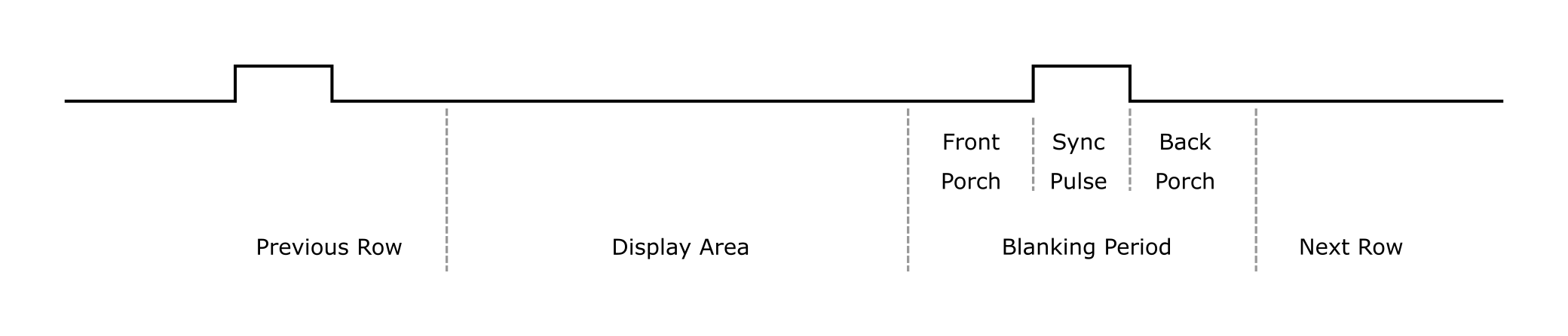
- The "front porch" - the number of pixels before the sync pulse
- Sync Pulse Width - the length of the sync pulse in pixels
- The "back porch" - the number of pixels after the sync pulse
Together the front porch, sync pulse and back porch are called the "blanking period" since during these periods color signals are ignored and don't affect the display.
The horizontal blanking periods mark the end of one row and the start of another while the the vertical blanks periods mark the end of one entire screen frame and the start of the next.
You might be wondering: if these are timing values then how "long" is a pixel?
For the horizontal timings, the length of a pixel is given by the frequency of the pixel clock which is part of the timing specification. For example for 800 x 600 it's 40MHz so each "pixel" is 1/40,000,000 of a second.
For the vertical timings, the length of a pixel is the length of one horizontal row. ie: (display area + front porch + back porch + sync pulse width) * length of 1 horizontal pixel.
To generate these timings the FPGA just needs a couple of position counters - one that counts horizontally for each pixel clock tick, and one that counts vertically for each completed row. The sync pulses are then simply generated based on whether the counter is between the sync pulse range.
The VGA timing component (source code) provides the following signals:
- Horizontal and vertical sync pulses
- The current horizontal and vertical pixel position
- A signal that indicates whether the current position is within either the horizontal or vertical blanking periods (as opposed the display area)
The range of position values go from the negative sum of the blanking period to 1 less than the display area. For example, consider the horizontal timing information for 800 x 600 @ 60Hz display:
- Display Area: 800
- Front Porch: 40
- Sync Width: 128
- Back Porch: 88
In this case the total blanking period is 40+128+88 = 256 so the horizontal position counter would go from -256 to 799.
By using negative numbers for the blanking period it makes it easier to determine when a new row is about to start. Often the pixel generation logic will need a couple of cycles to work out the color of a pixel - which is easier when the two pixels before always have an index of -2 and -1 regardless of display resolution.
Testing the VGA Timing Component
I tested the VGA timing component with a simulation test bench (source code). To reduce the size of the simulation I made up a fake screen resolution of 20 x 20 pixels with all porch and pulse times set to 5 pixels.
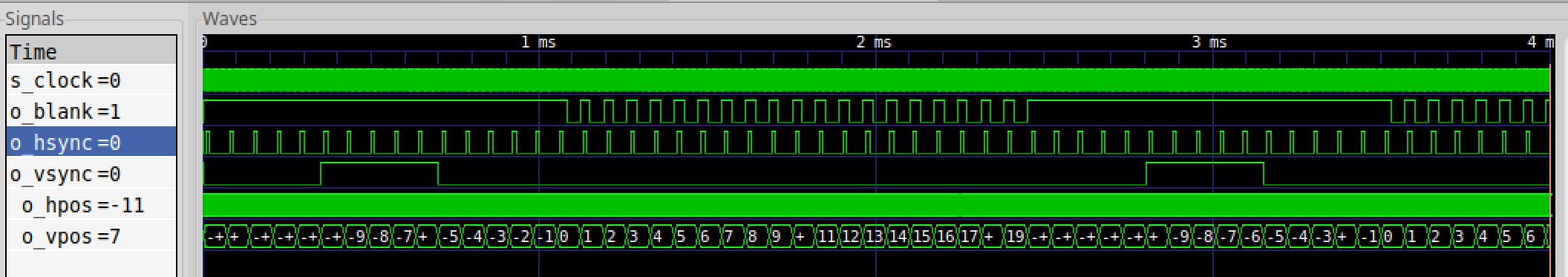
(In retrospect I should have used different values for each of the porch and pulse widths to make sure they're all being independently generated correctly).
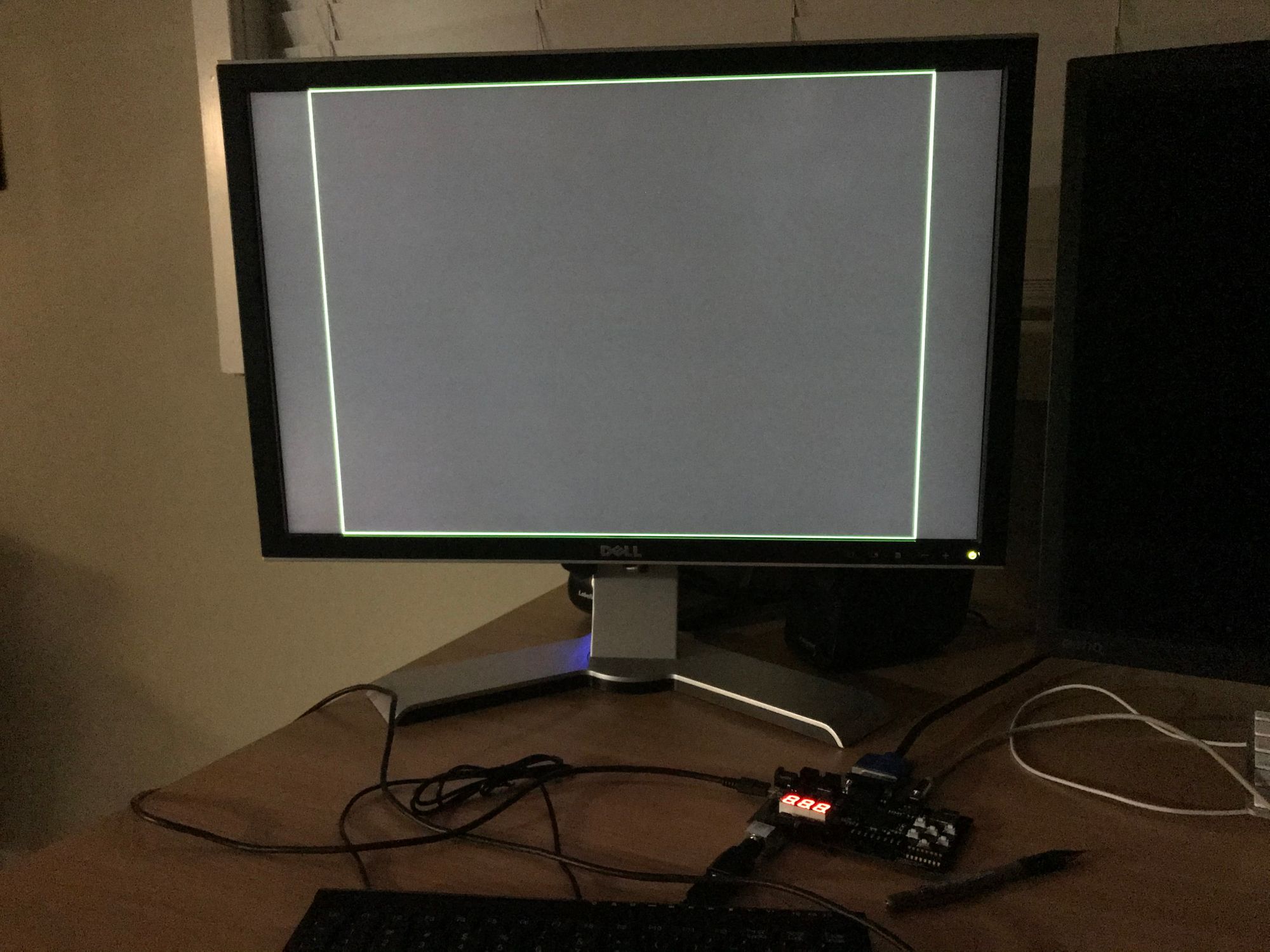
Once I was satisfied that it was working in the simulator, I setup a simple project to run on the FPGA that simply draws the boarder of the screen (source code). Here it is running on the FPGA - not terribly exciting but confirms the timing is correct.
TRS-80 Pixel Generation
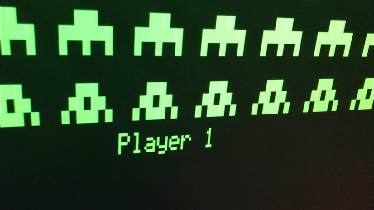
The TRS-80 has a monochrome 64 x 16 character display where each character cell is 6 x 12 pixels and each pixels has an aspect ratio of 2:3 - which can be achieved by pixel doubling horizontally and row tripling vertically.
The brings the total display resolution to 768 x 576. If you lookup the VGA timing details you'll find there's a VGA specification for exactly this resolution however it didn't work with my monitor. So I rounded up to 800 x 600 which is a far more common resolution and works fine.
Pixels values are sent to the monitor through three signals where the voltage levels control the red, green and blue level of the pixel currently being displayed. So all we need to do is generate the right voltage levels for the current pixel (as reported from the VGA timing component) and pixels will appear.
For a TRS80, what's on the screen at any moment is determined by two things:
- 1K of video memory that stores the character at each character position.
- A character ROM that defines the pixels that make up each character shape.
Since there are two memory read cycles involved, we need to work in advance by two clocks cycles:
- Two clock cycles before a pixel needs to be displayed the character is read from the video memory. We'll get the character back on the next clock cycle.
- One cycle before: use the character retrieved by the previous cycle to look up the character ROM. We'll get back the pixel bits on the next clock cycle.
- On the cycle the pixel is actually displayed we'll have the bits pattern for that pixel and we can generate the appropriate pixel color.
Note that these operations are pipe-lined: on any particular clock cycle we'll be working on three pixels all at once - the current pixel, the next pixel and the pixel after that.
The first thing we need to work out is the address in the video RAM for the current pixel. Unfortunately this can't be easily determined from the position reported by the VGA timing component since we need to divide by 6 horizontally and 12 vertically. If it was 8 and 16 it would have be easy since we could use bit shifting to divide by powers of two. 6 and 12 are a pain.
The solution is to use divide counters to constantly track which character cell we're currently in, which pixel within that cell and how many times we've repeated the pixel (ie: the pixel doubling/row tripling for the aspect ratio). The bulk of the logic in the video controller is just maintaining these counters (source code).
Once we've got the character row and column it's pretty easy to work out the video RAM address since the following formula can be calculated with simple bit shifting:
video RAM Address = row * 64 + column
The character ROM is implemented by defining the pixel patterns in VHDL with each character defined as 16-rows of 6-bit values. The character ROM was generated using a simple NodeJS script that reads a binary ROM file and generates the appropriate VHDL code.
Even though each character cell is only 12 rows high, arranging the character ROM in rows of 16 simplifies the calculation of the ROM address:
character ROM address = characterNumber * 16 + rowInCharacterCell
Once we get back the 6 bits that define that row in the character cell, we just need to pick out the appropriate pixel value for the current horizontal pixel within the cell.
Testing the Video Controller
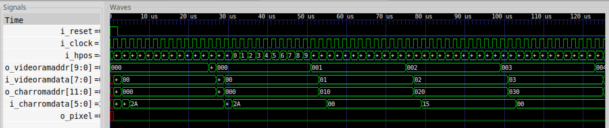
Again, I tested this in the simulator (source code). In this signal trace, you can see the staggered two pixel cycles used for each pixel:
To test on the FPGA, rather than using actual video RAM and having to populate it somehow, I simply implemented a fake RAM that returns a character based on the address requested. (source code)
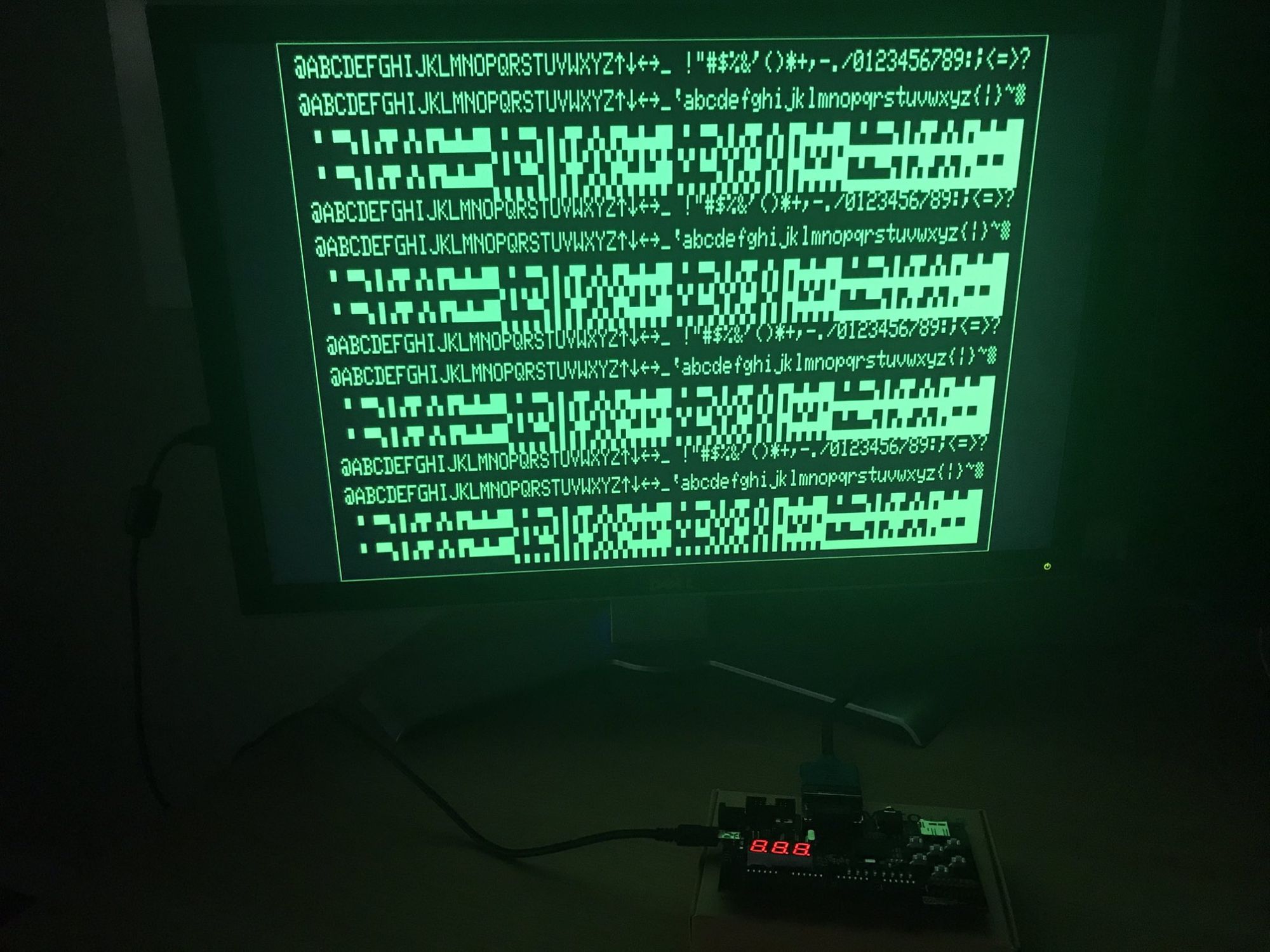
That's it! I now had a working TRS-80 video controller!
Generating Colors
You might be wondering how the FPGA generates the varying voltage levels for the red, green and blue channels to produce colors - after all the FPGA is a digital device that works in binary right?
The answer is pretty simple: the FPGA board has multiple digital pins connected through a resister ladder that generates different voltages. The Mimas V2 board I'm using for this project has 8 bit color so there are three pins for red, three for green and 2 for blue.
The TRS-80 video controller maps lit pixels to green to simulate the classic old-school green screen monitor.
Thinking About Clocking
In FPGA designs it's always a good idea to avoid multiple clock domains - ie: different parts of the design running at different clock frequencies. When a signal crosses between clock domains it needs to be synchronized which makes working with multiple clock domains a pain.
One way to avoid multiple clock domains is to use a higher frequency master clock and divide it to lower frequencies using a "clock enable" signal that indicates if the current clock cycle is "active" for a particular required frequency. With this approach everything is running on the same master clock but different parts of the design are only active every Nth cycle.
So what are the clocking requirements for this project?
- As mentioned above the 800 x 600 @ 60Hz VGA resolution requires a 40MHz pixel clock.
- The TRS-80's Z-80 CPU runs at 1.774MHz
- SD cards can run at up to 400KHz
- SDHC cards can run up to 25MHz
So I was thinking about all this and just stumbled upon this co-incidence...
- 80MHz divided by 2 gives the 40MHz for the video controller
- 80MHz divided by 45 gives 1.777MHz for the CPU
- 80MHz divided by 200 gives 400KHz for SD cards
- 80MHz divided by 4 gives 20MHz for SDHC cards
That 1.777MHz is shockingly close to 1.774 and 20MHz for the SDHC card is plenty fast enough for what will be needed. Given the how much simpler things are on a single clock domain that's what I'm going to run with.
(You'll notice in the test projects for the video controller everything is running at 80MHz with a clock enable for every second cycle - that's why)
Stay tuned... details on the keyboard controller coming soon.
Have thoughts on this? Leave a comment on Twitter.